Previous Year Questions
Admission syllabusComputer Science and Engineering
430 questions8. A 4-pole, 3-phase induction motor operates from a supply whose line voltage is 440V. Rotor speed is 1440 r.p.m. when the slip is 0.04. If a two pole synchronous motor is connected to the same supply what will be the speed of the synchronous motor. (13) [একটি ৪ পোল, ৩-ফেজ ইনডাকশন মোটর ৪৪০ ভোল্ট supplyএ চলে। ০.০৪ স্লিপে মোটরটির রোটার স্পীড ১৪৪০ আর.পি.এম.। যদি একটি দুই পোলের সিনক্রোনাস মোটরকে একই supply এ সংযুক্ত করা হয় তবে সিনক্রোনাস মোটরের স্পীড কত হইবে? (13)]
Answer & solution / উত্তর ও সমাধান
\[N_s=\frac{1440}{1-0.04}=1500\,\mathrm{rpm},\quad f=\frac{PN_s}{120}=50\,\mathrm{Hz}\]
\[N_{s,2}=\frac{120(50)}2=\boxed{3000\,\mathrm{rpm}}\]
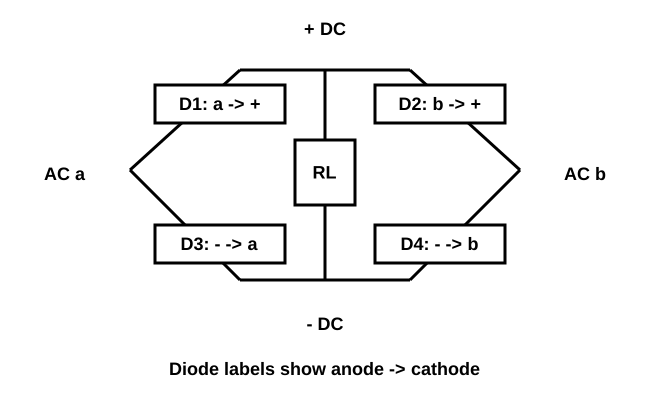
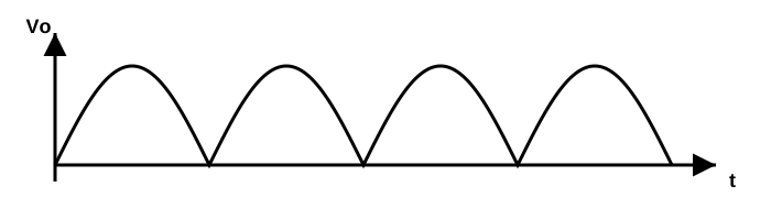
9. Draw a circuit diagram of a full-wave bridge rectifier and its output voltage wave form. What are the advantages of this rectifier over 2-diode full-wave rectifier? [আউটপুট ভোল্টেজ ওয়েভফর্ম সহ একটি ফুল-ওয়েভ ব্রীজ রেকটিফায়ারের সার্কিট চিত্র অংকন কর। ২-ডায়োড ফুল-ওয়েভ রেকটিফায়ারের তুলনায় এই রেকটিফায়ারের সুবিধাসমূহ কি?] (13)
Answer & solution / উত্তর ও সমাধান
চার diode bridge-এর দুই AC terminal source-এ, DC +/− terminal load-এ। Positive half-cycle-এ এক diagonal pair এবং negative half-cycle-এ অন্য pair conduct করে; load current একই দিকে থাকে।
\[v_o\approx|V_m\sin\omega t|,\quad V_{DC}=2V_m/\pi\]
Center-tapped 2-diode rectifier-এর তুলনায় center tap লাগে না এবং একই output peak-এর জন্য diode PIV কম; তবে একসঙ্গে দুটি diode drop থাকে।
10. Showing the active, cutoff and saturation regions, sketch the output characteristics of a common base n-p-n Si transistor. State the biasing conditions for each. [একটি কমন বেস এন-পি-এন সিলিকন ট্রানজিস্টরের আউটপুট ক্যারেক্টারেস্টিকস আঁক এবং অ্যাকটিভ, কাটঅফ ও স্যাচুরেশন নির্দেশ কর। প্রতি ক্ষেত্রে বায়াসিং এর শর্তাবলী উল্লেখ কর।]
Answer & solution / উত্তর ও সমাধান
| Region | Emitter-base junction | Collector-base junction |
|---|---|---|
| Active | Forward biased | Reverse biased |
| Cutoff | Not forward biased | Reverse biased |
| Saturation | Forward biased | Forward biased |
Common-base output graph-এ x-axis VCB, y-axis IC, প্রতিটি curve fixed IE-এর জন্য। Active region-এ IC ≈ αIE + ICBO; NPN-এর VCB > 0। VCB < 0 হয়ে collector-base forward biased হলে saturation; IE ≈ 0 হলে cutoff curve।
11. (a) A sinusoidal voltage, $v = 30\sqrt{2} \sin 314t$ volts is applied to the input of the circuit shown in Fig. 4. Draw the wave form of the output voltage. [সার্কিটের ইনপুটে একটি সাইনোসয়ডাল ভোল্টেজ প্রয়োগ করা হইল। আউটপুট ভোল্টেজের ওয়েভ ফর্ম আঁক] (07)
Fig. 4 Circuit Diagram:
An input AC voltage source $v$ connected in series with a $5\text{ k}\Omega$ resistor.
A clipper network connected across the output $V_o$:
One branch has a diode pointing downwards in series with a $10\text{ V}$ DC source (positive terminal up).
The parallel branch has a diode pointing upwards in series with a $10\text{ V}$ DC source (negative terminal up).
Incomplete source data
Answer & solution / উত্তর ও সমাধান
মূল চিত্র/ডেটা অসম্পূর্ণ: এই document-এ নির্ভরযোগ্য original circuit image ও সম্পূর্ণ সংযোগ নেই। তাই একক numerical answer নিশ্চিত করা যাচ্ছে না।
\[V_m=30\sqrt2\approx42.426\,\mathrm V,\quad f=314/(2\pi)\approx50\,\mathrm{Hz}\]
Output waveform-এর clipping level ও polarity diode direction, bias source এবং output terminals-এর ওপর নির্ভর করে। শুধু input sine wave থেকে output নির্ধারণ সম্ভব নয়।
11. (b) Show how a MOSFET can be operated as an amplifier. [দেখাও যে, MOSFET একটি অ্যামপ্লিফায়ার হিসাবে কাজ করিতে পারে।] (07)
Answer & solution / উত্তর ও সমাধান
N-channel enhancement MOSFET common-source amplifier-এ source ground, drain resistor RD দিয়ে VDD-তে, gate DC divider দিয়ে bias করো। Input/output coupling capacitors DC block করে।
\[V_{GS}>V_T,\quad V_{DS}\ge V_{GS}-V_T\]
এই saturation-region Q-point-এর চারপাশে ছোট gate signal drain current পরিবর্তন করে।
\[v_o\approx-g_m(R_D\parallel R_L\parallel r_o)v_{gs}\]
Negative sign 180° phase inversion বোঝায়। MOSFET saturation হলো amplification region, BJT saturation-এর মতো নয়।
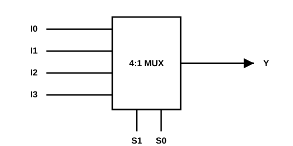
12. A logic circuit has three inputs and one output. The output is 1 when at least two inputs are 1. Implement the logic circuit with a $4 \times 1$ MUX and necessary logic gates. [একটি লজিক সার্কিটের তিনটি ইনপুট এবং 1টি আউটপুট আছে। আউটপুটের মান ১ হয় যখন কমপক্ষে দুইটি ইনপুট ১ হয়। একটি $4 \times 1$ MUX এবং প্রয়োজনীয় লজিক গেইট ব্যবহার করিয়া লজিক সার্কিটটি তৈরি কর।] (13)
Answer & solution / উত্তর ও সমাধান
\[F=AB+AC+BC\]
4:1 MUX-এ select S1 = A, S0 = B নাও।
| AB | F | MUX data input |
|---|---|---|
| 00 | 0 | I0 = 0 |
| 01 | C | I1 = C |
| 10 | C | I2 = C |
| 11 | 1 | I3 = 1 |
এই সংযোগে output ঠিক তখন 1 হবে, যখন তিন input-এর অন্তত দুটি 1। অতিরিক্ত gate প্রয়োজন নেই।
13. Write a program to find the sum of all the odd integer numbers from 1 to 99. (Use C or FORTRAN] [C অথবা FORTRAN ব্যবহার করিয়া ১ হইতে ৯৯ পর্যন্ত সমস্ত বিজোড় সংখ্যার যোগফল বাহির করার জন্য একটি প্রোগ্রাম লিখ।] (14)
Answer & solution / উত্তর ও সমাধান
#include <stdio.h>
int main(void) {
    int sum = 0;
    for (int i = 1; i <= 99; i += 2) sum += i;
    printf("%d\n", sum);
    return 0;
}
\[1+3+\cdots+99=50^2=\boxed{2500}\]
14.(a) What is the difference between a data and an information? List the name of six BDMS packages. [ডাটা ও তথ্যের মধ্যে পার্থক্য কি? ছয়টি BDMS প্যাকেজের নাম লিখ।]
Answer & solution / উত্তর ও সমাধান
Data হলো raw facts; information হলো context ও processing-এর ফলে অর্থবহ data। উদাহরণ: 70, 80, 90 raw marks; average 80 একটি তথ্য।
ছয়টি DBMS: PostgreSQL, MySQL, MariaDB, SQLite, Oracle Database, Microsoft SQL Server।
14. (b) What is meant by LAN and WAN in computer networking? [কম্পিউটার নেটওয়ার্কিং এ LAN এবং WAN বলিতে কি বুঝায়?] (07)
Answer & solution / উত্তর ও সমাধান
| Network | পরিসর | সাধারণ বৈশিষ্ট্য |
|---|---|---|
| LAN | Room/building/campus | সীমিত area, সাধারণত এক প্রতিষ্ঠানের নিয়ন্ত্রণ |
| MAN | City/metropolitan area | একাধিক LAN সংযোগ |
| WAN | Region/country/world | দূরবর্তী network যুক্ত; carrier infrastructure ব্যবহার হতে পারে |
15. Write down the task of the following instructions of 8085 microprocessor. [8085 মাইক্রোপ্রসেসরের নিম্নলিখিত ইন্সট্রাকশন গুলির কাজ লিখ।]
(i) STA 16-bit Address, (ii) INR M, (iii) CMA, (iv) JC 16-bit Address, (v) RET (14)
Answer & solution / উত্তর ও সমাধান
| 8085 instruction | কাজ |
|---|---|
| STA address | A-এর byte নির্দিষ্ট 16-bit memory address-এ store |
| INR M | HL নির্দেশিত memory byte 1 বাড়ায়; CY অপরিবর্তিত |
| CMA | A-এর প্রতিটি bit complement; flags অপরিবর্তিত |
| JC address | CY = 1 হলে address-এ jump |
| RET | Stack থেকে saved return address PC-তে নিয়ে subroutine থেকে ফেরে |
1. With the help of Thevenin’s theorem, calculate the current flowing through the $3\ \Omega$ resistor in the following network. [নিম্নের নেটওয়ার্কে থেনেনিন থিওরেম প্রয়োগ করিয়া ৩ ওহম রেজিস্টরের মধ্যে প্রবাহিত কারেন্ট বাহির কর।] (10)
Circuit Diagram:
A $24\text{ V}$ source connected to a $4\ \Omega$ series resistor, leading to an $8\ \Omega$ top branch resistor.
A parallel branch featuring a $2\text{ A}$ current source (pointing upwards) connected in parallel with a $4\ \Omega$ resistor between nodes C and D.
A $6\ \Omega$ top branch resistor leads to terminal A.
The load resistor is $3\ \Omega$ connected across terminals A and B, with a load current $I_B$.
Incomplete source data
Answer & solution / উত্তর ও সমাধান
মূল চিত্র/ডেটা অসম্পূর্ণ: এই document-এ নির্ভরযোগ্য original circuit image ও সম্পূর্ণ সংযোগ নেই। তাই একক numerical answer নিশ্চিত করা যাচ্ছে না।
- Load resistor সরিয়ে terminal open-circuit voltage Vth বের করো।
- Independent voltage source short এবং independent current source open করে terminal resistance Rth বের করো; dependent source থাকলে রেখে test-source method ব্যবহার করো।
- Load পুনরায় যুক্ত করে নিচের সূত্রে current নির্ণয় করো।
\[I_L=\frac{V_{th}}{R_{th}+R_L}\]
Source solution-এর সংখ্যা যাচাই করতে original circuit, source polarity ও load label প্রয়োজন।
2. Find the reading of the voltmeter in the following circuit. [নিম্নের সার্কিটে ভোল্টমিটারের পাঠ বাহির কর।] (08)
Circuit Diagram:
A $10\text{ V}$ DC source supplying a bridge/parallel network.
Top branch contains a $5\ \Omega$ resistor connected in series with a voltmeter (V) between nodes A and B.
The middle parallel branch contains a $6\ \Omega$ and a $2\ \Omega$ resistor in series.
The bottom return branch contains a $2\ \Omega$ resistor.
Incomplete source data
Answer & solution / উত্তর ও সমাধান
মূল চিত্র/ডেটা অসম্পূর্ণ: এই document-এ নির্ভরযোগ্য original circuit image ও সম্পূর্ণ সংযোগ নেই। তাই একক numerical answer নিশ্চিত করা যাচ্ছে না।
Reference node নিয়ে KCL/KVL বা nodal equations solve করতে হবে; তারপর VAB = VA − VB। Ideal voltmeter infinite resistance ধরে current নেয় না। A/B-এর অবস্থান ও source polarity ছাড়া voltage-এর মান/sign নির্ধারিত নয়।
3. Write the equilibrium equations for the following network on nodal basis and obtain the voltages $V_1, V_2, V_3$. All the resisters are of $1\ \Omega$. (08) [নোড ভোল্টেজ প্রক্রিয়ায় নিম্নের নেটওয়ার্কের ভারসাম্য সমীকরণ লিখ এবং $V_1, V_2, V_3$-এর মান নির্ণয় কর। প্রতি রেজিস্টারের মান $1\ \Omega$ ।]
Circuit Diagram:
A $10\text{ V}$ DC voltage source connected to resistor $R_1$ leading to node $V_1$.
Node $V_1$ has a shunt resistor $R_2$ to ground and connects to node $V_2$ via resistor $R_3$.
Node $V_2$ has parallel shunt branches with resistors $R_4$ and $R_5$ to ground, and connects to node $V_3$ via resistor $R_6$.
Node $V_3$ has parallel shunt branches with resistors $R_7$ and $R_8$ to ground.
Incomplete source data
Answer & solution / উত্তর ও সমাধান
মূল চিত্র/ডেটা অসম্পূর্ণ: এই document-এ নির্ভরযোগ্য original circuit image ও সম্পূর্ণ সংযোগ নেই। তাই একক numerical answer নিশ্চিত করা যাচ্ছে না।
\[\sum_{j\text{ connected to }i}\frac{V_i-V_j}{R_{ij}}=I_{i,\mathrm{injected}}\]
প্রতিটি 1 Ω branch-এ current = Vi − Vj ampere। তিন node-এর conductance matrix G তৈরি করে GV = I solve করো। কোন nodes connected এবং source directions না জানলে matrix নির্ধারিত নয়।
4. (a) The power factor in an ac circuit is 80% lagging, explain briefly. [একটি এসি সার্কিটে পাওয়ার ফ্যাক্টর ৮০% ল্যাগিং বলিতে কি বুঝ তাহা লিখ।] (04)
Answer & solution / উত্তর ও সমাধান
\[\cos\phi=0.8,\quad\phi=\cos^{-1}(0.8)=36.87^\circ\]
Sinusoidal circuit-এ current voltage-এর থেকে 36.87° পিছিয়ে থাকে; real power apparent power-এর 80%।
4. (b) Mention the disadvantages of low power factor in a circuit. [এসি সার্কিটে কম পাওয়ার ফ্যাক্টরের অসুবিধাসমূহ উল্লেখ কর।] (04)
Answer & solution / উত্তর ও সমাধান
একই real power ও supply voltage-এ কম power factor মানে বেশি current। এতে \(I^2R\) loss, voltage drop ও required conductor/transformer kVA rating বাড়ে; system capacity কম কার্যকরভাবে ব্যবহৃত হয়।